


Taking a closer look
Sophisticated microscope elevates UD research capability


5:33 p.m., Oct. 27, 2011--University of Delaware Prof. John Xiao is researching ways to make tiny electronics devices – such as those found in computer hard disks and memories, environmental sensors; even iPods – perform faster and consume less energy.
His work involves using spin electronics, or “spintronics,” an emerging science that focuses on harnessing the “spin,” or magnetic properties of electrons, to encode and process data.
Research Stories

Chronic wounds
Prof. Heck's legacy
This high-tech work requires fabricating devices and looking at the atomic structure of materials at the nanoscale in order to determine how they are organized, and then investigating how materials can be improved or enhanced to impact performance (speed) and energy use (consumption).
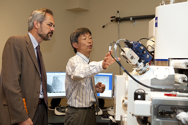
Xiao, a professor of physics and astronomy in the College of Arts and Sciences, is one of several UD researchers who are excited about the arrival of a new, sophisticated microscope to campus Thursday, Oct. 27.
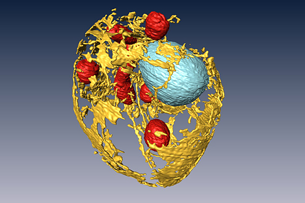
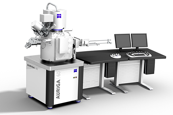
The instrument, called the Zeiss AURIGA CrossBeam microscope, is a dual beam focused ion beam and scanning electron microscope (FIB-SEM) capable of both nanoscale deposition and machining. It will provide high-resolution imaging and a wide variety of analytical capabilities, enabling research for both soft and hard materials including polymers, biomaterials, ceramics, metals, semiconductors, composites and more.
“Much of my research uses transmission electron microscopy (TEM), where we take pictures of atoms within a multilayer structure to view how atoms in each layer are arranged in order to understand the structural-property relationship of the materials,” explained Xiao.
“In order to use TEM to see our specimen, the materials we put under the microscope must be very thin, on the order of a nanometer or one billionth of a meter. The Zeiss microscope allows for ion beam etching, which is a faster way to expose the vertical wall, or cross section, and view the structure’s multiple layers.”
The microscope is designed to derive maximum information out of a material sample using advanced analytics. For materials analysis, researchers can create 3D imaging and analysis of non-conducting materials, patterning of complex nanostructures and high resolution ion imaging, as well as simultaneous detection of topographical and compositional information. Since the microscope also allows material to be deposited, it opens to the door for designing and creating entirely new structures in the lab at the nanoscale.
The instrument is the first major acquisition for the 194,000-square-foot Interdisciplinary Science and Engineering Laboratory (ISE Lab) now under construction at UD. Temporarily installed in Spencer Laboratory, the microscope is available to all members of the University community, as well as UD partners in industry, government and academia.
“DuPont uses electron microscopy in its advanced materials product development for many different sectors, including agriculture, transportation, alternative energy, electronics, construction and packaging. In particular, we would use this instrument to help understand polymer/metal interfaces and polymer/semiconductor interfaces,” said Barbara Wood, senior research associate at DuPont Central Research.
Darrin J. Pochan, professor of materials science and engineering, said he plans to use the Zeiss FIB-SEM microscope to characterize and engineer nanostructure and materials through the assembly of molecules in solution.
“One area we focus on is the assembly of soft materials from peptides that are excellent candidates for the delivery of drug therapies or the regeneration of diseased tissues inside the body,” Pochan explained.
“While we currently control the nanostructure of these and other materials through the proper design of the molecules that make them, we would like to be able to further pattern these materials on the nanoscale with FIB after they have been assembled and formed, in order to fine-tune the nanostructure present for desired interactions with living systems,” he continued.
Andrew Teplyakov, professor of chemistry and biochemistry, believes the new microscope offers unique advantages not previously available on campus.
“Imaging at the nanoscale requires atomic precision. This specific type of microscopy is a true necessity to look at the nanostructures or thin films and their interface with support material,” he said.
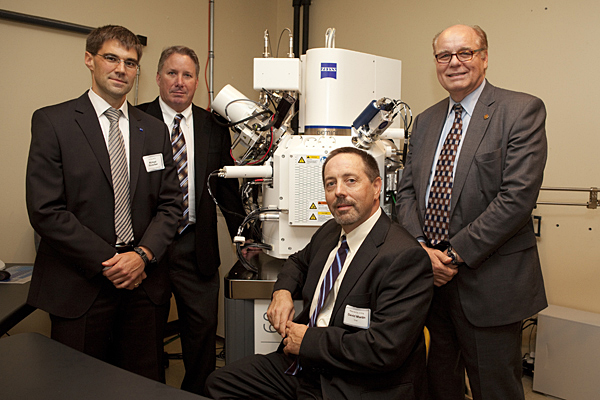
Representatives from UD, Carl Zeiss, Inc., industry and academia gathered to celebrate the instrument’s arrival on campus Oct. 27 at the Center for Composite Materials.
"Carl Zeiss has enjoyed a long relationship with the University of Delaware. I was very pleased to celebrate their purchase of our Auriga 60 CrossBeam almost exactly 10 years after our first CrossBeam tool was shipped to the U.S. Carl Zeiss looks forward to continuing our relationship and supporting the research and scientific discoveries that are uncovered from this system," said James A. Sharp, president of Carl Zeiss Microscopy, LLC.
“This instrument is an excellent example of the opportunities that will be provided by the ISE-Lab, including the ability to produce valuable research results,” concluded David C. Martin, chair of the Department of Materials Science and Engineering.
Article by Karen B. Roberts
Photos by Ambre Alexander