


A big day for tiny tech
Work now underway in UD's new Nanofabrication Facility


1:46 p.m., March 10, 2016--You have to think small to do the kind of work now underway in the University of Delaware's new Nanofabrication Facility (UDNF).
But you have to think big, too, because what happens in the UDNF "clean room" – more on that later – won't stay in the clean room. It will ship out to the wide world of biology, chemistry, engineering, electronics, health care, manufacturing, energy, physics, and who-knows-where-else.
Research Stories
Chronic wounds
Prof. Heck's legacy
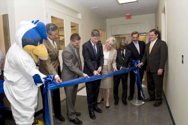
Tuesday, UD officials, faculty, staff and students marked the opening of the $30 million "machine shop of the 21st century" with a keynote address by nanotechnology pioneer Harold Craighead of Cornell University and a ceremonial ribbon-cutting in a packed hallway on the first floor of the Harker Interdisciplinary Science and Engineering Laboratory.
The facility is equipped to produce devices that cannot be seen by the naked eye – materials that can be used in a wide array of applications from medicine to environmental sciences to solar energy harvesting. The equipment in the laboratory will allow researchers to make devices as small as 10 nanometers. For reference, there are 10 million nanometers in one centimeter.
"This is a state-of-the-art facility that will allow faculty, staff, students, and collaborators from across campus and beyond to envision research at its smallest scale," said Charlie Riordan, deputy provost for research and scholarship. "There are tremendous opportunities to develop technologies at the atomic level. And we are very well poised for all disciplines to leverage this technology to address the grand challenges we face in society."
The facility was years in the planning and now is in the hands of co-directors Matthew Doty, associate professor of materials science and engineering, physics, and electrical and computer engineering, and John Xiao, Unidel Professor of Physics and Astronomy. Xiao specializes in spintronics, nanofabrication and magnetic materials. Doty studies and develops nanostructured semiconductors.
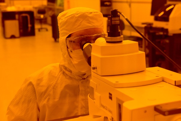
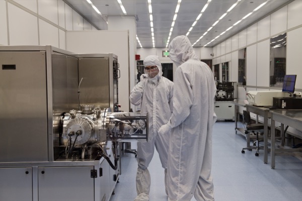
Though the symbolic ribbon was cut Tuesday, you can't just walk into this workshop. Entry to the 8,500-square-foot clean room, where all the work is done, requires training, credentials, painstaking protocols and coverage from the "gowning room" – including hair nets, face and head covers, jumpsuits, gloves, booties, safety glasses and hard hats.
The "clean" referenced here isn't the white-glove kind of clean. It's far to the extreme of that. The clean room is rated for two layers of clean – one is Class 100, which means that it has no more than 100 particles measuring 500 nanometers or more in a cubic foot of air, and the other is Class 1,000, which means it has no more than 1,000 such particles per cubic foot.
For reference, an ordinary room would register about 100,000 particles per cubic foot.
To keep the air this clean, the air in the room is constantly pushed through filters, changing the air up to 300 times an hour.
Such hyper-clean conditions are mandatory because work at nanometer length scales can be sabotaged by unwanted particles. Without such measures, Xiao said, it would be like trying to frost a wedding cake while someone is throwing basketballs at you.
The clean room has four separate bays for processes including lithography, deposition of thin films, etching, and thermal processing.
Several doctoral candidates – including Xiangyu Ma, Jimmy Hack, and Sarah Geiger – were at their nanofab stations Tuesday, properly suited up with their clean-room gear.
"We're getting the tools up and running and they're helping us qualify the tools," said Scott McCracken, facility specialist. "They're starting to do some work as well, starting some of their own projects."
Ma, whose adviser is Doty, said his research includes development of new semiconductors for future generations of computers. Hack has been using a device called a magnetron sputterer to ionize particles, which helps to deposit material onto silicon. And Geiger is working with organic photoresist, which will be used in microfluidics and biomaterials.
"We're all really excited," Ma said.
The nanofabrication technology makes the University more appealing to students and faculty with such interests, and George Watson, physicist and dean of the College of Arts and Sciences, said he is taking the opportunity to recruit new faculty.
"This is opening up new opportunities," he said.
Ira Winston, chief infrastructure officer at the University of Pennsylvania's School of Engineering and Applied Science, saluted UD's accomplishment and that of his former colleague, Iulian Codreanu, who is now operations director of UDNF.
"We thought we built the premiere facility," Winston said. "But they [UD] made some choices we didn't make. They have some things we don't. So I know some of our users will be coming here. Collaboration is going to happen. We have some things they don't and they have some things we don't."
Industry leaders have shown significant interest in the University's new capacity, too. It's expensive equipment – the electron beam lithography setup alone cost about $3 million.
Jim Sharp, president of Carl Zeiss Microscopy, was on hand for the ribbon cutting. The facility has several Zeiss instruments in it.
"The future of science is in the fab," Sharp said. "The science will go there."
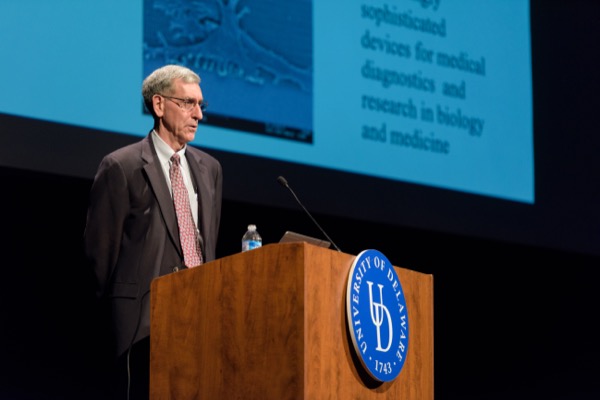
In his address at Mitchell Hall on Tuesday afternoon, Craighead pulled the curtain back a bit to explain how nanofabrication already has transformed research and development.
The former director of the National Nanofabrication Facility at Cornell and founding director of Cornell's Nanobiotechnology Center studies such things as single molecule biophysics, chemical sensors, and the physics of nanoelectromechanical systems.
He showed how a plant pathologist used the technology to better understand the development of bean-rust fungus by engineering surfaces for experiments. He sketched out the study of engineered surfaces for neuroscience, and described his analysis of individual molecules, including DNA sequencing.
In health care, physicians may one day gain access to a "lab-on-a-chip" – a testing device that allows sample materials and data to be analyzed in an office or in the field, not requiring a trip to a lab.
"This technology can bring people together from different disciplines together in ways they never would have done before," he said.
No one can see such minutia with their eyes or even a conventional microscope. One nanometer is about 100,000 times smaller than the diameter of a human hair. But with photolithography, scanning electron microscopy and other instruments, scientists can manipulate these miniscule materials to produce significant devices and analytical processes for many different purposes.
"I'm only scratching the surface regarding what is possible today," Craighead said. "There will be applications we can't envision now. I am unable to predict the future.... I can certainly predict it's going to have impact, but I can't predict where."
It is because of nanoscale technology that sophisticated computing can be done on devices the size of a wristwatch or cell phone rather than the massive machines that once required entire rooms to do the work of a glorified calculator.
And now, UD's tiny tech machine shop is poised to deliver extraordinary new possibilities.
"Things are already up and running," Doty said. "We're ready for business."
Article by Beth Miller
Photos by Evan Krape and Lane McLaughlin
Video by Robert DiIorio