


Heat waves
Research team reports new approach to simulating nanoscale heat transfer


10:52 a.m., April 6, 2016--Thermoelectric materials, which can directly and reversibly convert heat to electrical energy, are used in a variety of applications, including cooling of electronic devices and waste heat energy conversion.
A persistent challenge associated with thermoelectric materials is efficiency — if they could be designed to more efficiently convert heat into electricity, the door would be opened to a wide range of practical applications.
Research Stories


Chronic wounds
Prof. Heck's legacy
To make them more efficient, the materials must act like a thermal insulator while electronically behaving like a conductor — a feature not often found in natural materials.
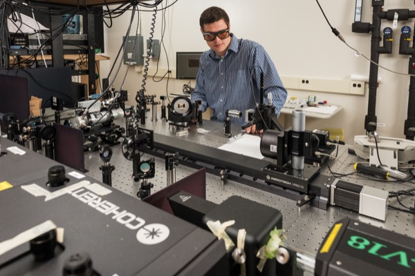
A research group led by Joe Feser, assistant professor in the Department of Mechanical Engineering at the University of Delaware, is investigating the limits of heat transport using a suite of new tools for nanoscale thermal measurement and simulation, with an eye toward the creation of materials that are more thermoelectrically efficient.
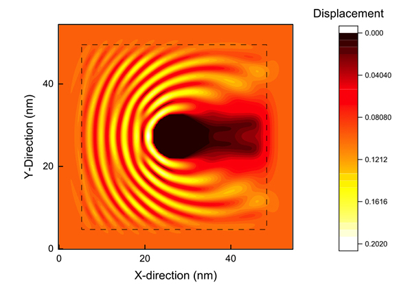
One common strategy employed by his group is the use of nanoparticles to scatter heat-carrying vibrations, known as phonons. The team is developing tools to study phonon scattering so that the size, shape, and composition of nanoparticles can be optimized for thermoelectric applications.
Feser and doctoral student Rohit Kakodkar recently reported a new approach to that problem in a paper, “A Framework for Solving Atomistic Phonon-Structure Scattering Problems in the Frequency Domain Using Perfectly Matched Layer Boundaries,” in the Journal of Applied Physics.
The new framework significantly reduces the amount of computational power needed to simulate phonon scattering and greatly increases the maximum size of the systems that can be studied using computers.
Feser explains that continuum mechanics models — which, for the sake of efficiency, ignore the fact that matter is made up of atoms — are traditionally used to explain phenomena like phonon scattering. However, while this approach is accurate enough on length scales greater than the distance between atoms, it may not be effective in characterizing the behavior of nanometer-length waves, which are often the wavelengths involved in heat transport.
The obvious solution is to have simulations that include an equation for each individual atom and track the behavior over an extended period of time, but that’s where the computational logjam occurs. Traditional techniques like molecular dynamics are too slow to simulate scattering for every heat-carrying vibration separately, and other existing techniques are limited in their ability to simulate large systems.
The atomistic model developed by Feser and Kakodkar can solve for a large number of atoms at a time. “Basically what we’ve done is remove the unnecessary physics and embed facts we already know about the solutions into the solution procedure,” Feser says.
Another important use for the new tool is that it has enabled researchers to settle longstanding controversies about how to describe the physics of phonons encountering interfaces — that is, whether they travel across coherently or scatter diffusely — and especially how disorder changes that. The framework also has the advantage that it can be scaled up for use with supercomputers, which are seeing increased use for complex simulations.
Ultimately, the goal is to have precise control over the design of new materials at the level of their tiniest constituents.
“The design of new materials that push the limits of achievable transport properties — i.e., thermal conductivity, interface conductance, heat capacity, and thermoelectric power factor — will enable the development of new device technologies based on these materials,” Feser says.
Article by Diane Kukich
Photo by Evan Krape