
 The University of Delaware is a nationally classified research institution. Founded in 1972, UD’s Institute of Energy Conversion (IEC) is the oldest solar research facility in the world and one of only two recognized as a Center of Excellence for Photovoltaic Research and Education by the U.S. Department of Energy.
The University of Delaware is a nationally classified research institution. Founded in 1972, UD’s Institute of Energy Conversion (IEC) is the oldest solar research facility in the world and one of only two recognized as a Center of Excellence for Photovoltaic Research and Education by the U.S. Department of Energy.
What we do
The Institute of Energy Conversion (IEC) develops the fundamental science and engineering required to improve photovoltaic device performance and processing technologies, and works to effectively transfer these laboratory results to large-scale manufacturing.

Solar Technologies
IEC’s broad scope of research and solar technologies spans the fields of physics, chemistry, materials science, electrical, chemical and mechanical engineering and more.
Cutting-Edge Facilities
Our outstanding talent, facilities and labs, and vast array of equipment allow for sophisticated research into thin-film based solar cells, photovoltaic systems and related engineering topics.
Industrial Collaboration
With 50 years of hands-on experience with photovoltaics, IEC has long been a go-to research and development resource.
Dedicated People
IEC is staffed by experienced professionals dedicated to serving the needs of our users — from state-of-the-art science academic research to resource development. We look forward to working with you!

Supporting research across UD
Collaboration across disciplines is a hallmark of research at UD and IEC is leading the way. Utilizing the groundwork laid by Dr. Karl Boer and his team, IEC is building upon their solid foundation while looking toward the future. More from the UD research community:

A Growing Need
“IEC was a trailblazer in another area,” said Larry Kazmerski, long-time director of Science and Technology at the National Renewable Energy Laboratory in Golden, Colorado. “It provided us with the first woman of solar energy. Maria Telkes made huge contributions in solar and did a lot in solar thermal storage. And this provided a pathway, recognizing that women should have a part in science as well.”

Job Creation
Job creation has been a key policy driver, said John Byrne, UD’s Distinguished Professor of Energy and Climate Policy, director of the Center for Energy and Environmental Policy and an affiliate of IEC.
“Solar creates more jobs per million dollars of investment — two to five times as many as other new electrical generation methods,” he said. “I’d love to say it was the zero-carbon footprint, but it was jobs.”
“Solar creates more jobs per million dollars of investment — two to five times as many as other new electrical generation methods,” he said. “I’d love to say it was the zero-carbon footprint, but it was jobs.”
The Future
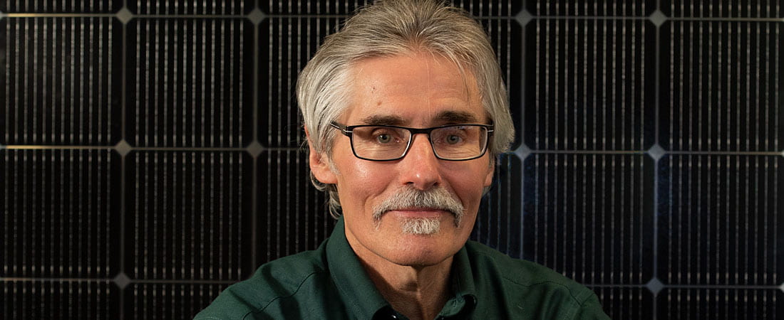
“What excites me about the future of IEC and solar research in general is that there is now a very strong and clear awareness of the need for renewable carbon-free energy,” said Steven Hegedus, senior scientist at IEC and a professor of electrical and computer engineering.
“There are billions and billions of dollars going into clean technology and solar is one of the biggest beneficiaries of that. The question is, can we get this all to happen quick enough to offset the worst effects of climate change that we’re headed toward?”
“There are billions and billions of dollars going into clean technology and solar is one of the biggest beneficiaries of that. The question is, can we get this all to happen quick enough to offset the worst effects of climate change that we’re headed toward?”

Leading the Way
The Institute for Energy Conversion (IEC) is led by Director William Shafarman, professor of materials science and engineering. The institute’s research focuses on making large-scale terrestrial power that is scalable, affordable and more reliable. Toward these goals, IEC is closely aligned with manufacturing companies, and the institute’s research projects have targeted manufacturing approaches. IEC is staffed by experienced professionals dedicated to serving the needs of our users.
Contact Us
If you need further assistance or have a specific request, please fill out the form below and we will get back to you shortly.